
Table of Contents
- Executive Summary: Key Takeaways for 2025–2030
- Technology Overview: Quasivacuum Thin Film Fundamentals
- Recent Innovations: Materials and Deposition Techniques
- Major Players & Industry Alliances (2025 Landscape)
- Market Size, Segmentation & Growth Projections to 2030
- Applications: Electronics, Optics, Energy & Beyond
- Investment Trends and Funding Hotspots
- Supply Chain Challenges and Solutions
- Regulatory & Environmental Considerations
- Future Outlook: Game-Changers and Strategic Roadmaps
- Sources & References
Executive Summary: Key Takeaways for 2025–2030
Quasivacuum thin film manufacturing is emerging as a disruptive process in materials science, offering a balance between the high purity of ultra-high vacuum deposition and the cost-effectiveness of atmospheric methods. As of 2025, the sector is witnessing accelerated adoption, driven by demand from electronics, photovoltaics, and advanced optics industries. The quasivacuum approach is particularly valued for its scalability and reduced equipment complexity, enabling broader commercial deployment.
Recent years saw a marked increase in the establishment of quasivacuum-compatible production lines, with major equipment suppliers such as Oxford Instruments and ULVAC expanding their portfolios to include systems tailored for this regime. The focus has shifted toward integrated deposition platforms capable of handling a variety of materials—metals, semiconductors, and organics—while maintaining the controlled environment required for high-performance thin films.
Data from ongoing partnerships, such as those between Applied Materials and leading display manufacturers, highlight that quasivacuum processes are reducing defect rates by up to 30% compared to legacy low-vacuum methods, while operating costs remain significantly lower than those of ultra-high vacuum systems. These improvements are spurring investments into pilot-scale facilities, with several large-scale rollouts anticipated across Asia and Europe in 2026–2027.
Material innovation is also accelerating. Companies like SINGULUS TECHNOLOGIES are introducing deposition sources and substrate transport mechanisms optimized for lower-pressure operation, targeting next-generation photovoltaics and transparent conductive films. Meanwhile, EV Group is advancing cluster tool architectures that combine quasivacuum deposition with in-line metrology, supporting real-time quality assurance.
The outlook for 2025–2030 is robust: as process reliability improves and cost barriers decline, quasivacuum thin film manufacturing is forecasted to capture significant share in markets such as flexible electronics, high-efficiency solar cells, and advanced sensors. Ongoing R&D, supported by cross-sector collaborations, is expected to yield new material stacks and device architectures only feasible in the quasivacuum regime.
- Scalable, lower-cost manufacturing is driving rapid commercialization.
- Major suppliers are expanding quasivacuum-focused equipment lines.
- Defect rates are declining and process integration is improving.
- Industry-wide adoption is expected to accelerate through 2030 as material and device innovations mature.
Technology Overview: Quasivacuum Thin Film Fundamentals
Quasivacuum thin film manufacturing represents a pivotal evolution in the field of thin film deposition, blending the advantages of traditional vacuum-based methods with the cost-effectiveness and scalability of lower-pressure processes. As of 2025, the focus within the industry is on refining processes that operate under partial vacuum—typically in the range of 10-1 to 10-3 mbar—rather than the ultra-high vacuum environments (10-6 mbar and below) traditionally used for atomic layer deposition (ALD) and physical vapor deposition (PVD).
This approach leverages the fact that many functional thin films, especially for applications in photovoltaics, flexible electronics, and barrier coatings, do not require the extreme cleanliness or atomic precision provided by ultra-high vacuum systems. Instead, quasivacuum deposition offers a practical balance between process control, material quality, and manufacturing throughput. The trend is particularly evident in the production of oxide, nitride, and organic thin films, where rapid scaling is needed to meet the growing demands of sectors like display technology and renewable energy.
Manufacturers are actively investing in equipment platforms optimized for quasivacuum conditions. For example, Bühler Group and Pfeiffer Vacuum have released modular coating systems that allow precise control of atmosphere and deposition parameters, supporting both reactive sputtering and plasma-enhanced chemical vapor deposition (PECVD) under partial vacuum. These systems are increasingly integrated with real-time process monitoring, leveraging in situ spectroscopy and feedback loops to ensure film uniformity and reproducibility at higher deposition rates.
In 2025, a central challenge is managing contaminants and maintaining film purity at lower vacuum levels. Companies such as Leybold are advancing pump and filtration technologies to minimize residual gases and particulates, thereby extending the application space of quasivacuum films to more demanding electronic and optical devices. Simultaneously, innovations in precursor chemistry—led by suppliers like Air Liquide—are enabling cleaner reactions and improved material properties even in less stringent vacuum regimes.
Looking ahead, the outlook for quasivacuum thin film manufacturing is robust. The ongoing shift toward sustainable manufacturing and the need for high-throughput, large-area deposition systems are expected to drive further adoption of these methods. The industry anticipates that, by 2027, quasivacuum processes will account for a growing share of functional coatings in applications such as flexible displays, advanced photovoltaics, and high-barrier packaging, as manufacturers prioritize cost, speed, and environmental impact without compromising product performance.
Recent Innovations: Materials and Deposition Techniques
Quasivacuum thin film manufacturing—where films are deposited under controlled low-pressure environments less stringent than ultrahigh vacuum—has seen notable advances in both materials and deposition techniques as of 2025. This approach is attracting growing interest for its balance between cost, scalability, and performance, especially in sectors such as flexible electronics, photovoltaics, and advanced coatings.
A significant development in recent years is the refinement of physical vapor deposition (PVD) and chemical vapor deposition (CVD) methods that operate efficiently in quasivacuum regimes. Companies such as ULVAC, Inc. have introduced new sputtering systems capable of high-uniformity film growth at pressures in the millitorr range. These systems are optimized for large-area coatings and are increasingly adopted in the display and solar industries, where throughput and uniformity are paramount.
On the materials front, the integration of complex oxides, nitrides, and chalcogenides in quasivacuum deposition is progressing rapidly. Advanced Micro-Fabrication Equipment Inc. (AMEC) has expanded its portfolio to include atomic layer deposition (ALD) tools specifically tailored for lower-vacuum operation, enabling the deposition of ultra-thin films with precise thickness control and excellent step coverage. These films are now being used in next-generation memory and logic devices.
In addition to traditional substrates, manufacturers are extending the range of compatible materials. Oxford Instruments recently showcased systems capable of depositing high-quality films on flexible substrates in quasivacuum environments, supporting the rise of bendable displays and wearables. This capability is crucial for the emerging market of flexible and stretchable electronics.
Looking ahead to the next few years, industry roadmaps point to further improvements in process control, in-situ monitoring, and hybrid techniques that combine elements of both vacuum and atmospheric deposition for enhanced material properties. Applied Materials, Inc. is investing in modular systems that allow rapid switching between different deposition atmospheres, providing manufacturers with increased flexibility and reduced downtime.
The outlook for quasivacuum thin film manufacturing is robust, with ongoing innovation focused on improving throughput, reducing energy consumption, and expanding the palette of functional materials. As equipment makers and material suppliers continue to refine their offerings, adoption across semiconductor, energy, and display sectors is set to accelerate through the remainder of this decade.
Major Players & Industry Alliances (2025 Landscape)
Quasivacuum thin film manufacturing, a key enabler for advanced electronics, optics, and energy devices, continues to evolve rapidly in 2025. The global industry is shaped by several major manufacturers and a growing web of strategic alliances, driven by the demand for high-performance coatings and next-generation semiconductor layers. Leading the sector are corporations with deep expertise in physical vapor deposition (PVD), chemical vapor deposition (CVD), and atomic layer deposition (ALD) technologies, which are adapted for quasivacuum process environments to optimize throughput and cost.
- Applied Materials, Inc. remains a dominant force in thin film deposition equipment, supplying advanced systems tailored for quasivacuum regimes. In 2025, the company has expanded its portfolio to address the scaling needs of sub-5nm semiconductor nodes, partnering with major foundries to accelerate integration into high-volume manufacturing.
- Lam Research Corporation continues to innovate in ALD and CVD platforms, introducing new modules aimed at enabling uniform thin films in lower-pressure, quasivacuum settings. Their collaborations with memory and logic device manufacturers are central to the proliferation of these techniques in the semiconductor supply chain.
- ULVAC, Inc., a leading Japanese supplier, has grown its international footprint through joint ventures and technology licensing. In 2025, ULVAC has focused on scaling up its batch and inline PVD tools for display and photovoltaic applications, where quasivacuum deposition is crucial for both performance and cost containment.
- Oxford Instruments plc remains a key player in research and pilot-scale systems, supporting both industrial partners and academic consortia. Their participation in EU and UK-based alliances in 2025 has accelerated the development of novel materials and process recipes for quantum and photonic devices.
Recent years have seen a rise in consortia and public-private alliances aimed at de-risking R&D and standardizing quasivacuum processes. For example, the SEMI industry association is facilitating roadmaps and pre-competitive collaborations, while companies such as Tokyo Ohka Kogyo Co., Ltd. are partnering with equipment suppliers to optimize precursor chemistries for large-area coatings.
Looking ahead, the industry is expected to witness further consolidation and cross-border partnerships, particularly as the demand for advanced thin films in areas like flexible electronics, advanced packaging, and solid-state batteries surges. Efforts to harmonize standards and share best practices, alongside significant investments in process automation, are likely to define the competitive landscape of quasivacuum thin film manufacturing through the remainder of the decade.
Market Size, Segmentation & Growth Projections to 2030
The global quasivacuum thin film manufacturing sector is entering a phase of accelerated growth as of 2025, driven by surging demand from key industries such as semiconductors, optoelectronics, photovoltaics, and advanced packaging. Quasivacuum processes—those conducted under reduced but not ultra-high vacuum—offer cost-efficiency and scalability compared to traditional high-vacuum deposition, making them increasingly attractive for a range of applications.
Market data from leading industry participants indicates that the quasivacuum thin film market is poised for robust expansion through 2030. For example, ULVAC, Inc., a prominent manufacturer of thin film production equipment, has reported intensified global interest in its quasivacuum sputtering and evaporation systems, particularly for displays, touch panels, and flexible electronics. Similarly, Advanced Micro-Fabrication Equipment Inc. (AMEC) has invested in new quasivacuum compatible platforms to address demand in memory, logic, and power device manufacturing, reflecting broader industry trends.
In terms of segmentation, the market is generally divided by application (e.g., microelectronics, energy, photonics), deposition method (sputtering, thermal evaporation, chemical vapor deposition), and end-user industry. The microelectronics and photovoltaic sectors currently command the largest share, but adoption in medical devices and automotive sensors is expected to show the fastest growth over the next five years. Notably, SINGULUS TECHNOLOGIES AG has reported increasing orders for its quasivacuum thin film systems for solar cell production, especially heterojunction (HJT) and perovskite technologies.
Geographically, Asia-Pacific remains the dominant region, led by China, Japan, and South Korea, where continued investment in semiconductor fabs and display panel production is driving sustained demand. However, North America and Europe are also seeing renewed activity, particularly as supply chain resilience and domestic manufacturing capacity become strategic priorities.
Looking ahead to 2030, most major equipment makers foresee compound annual growth rates (CAGR) ranging from 7% to 11% for quasivacuum thin film manufacturing. This outlook is underpinned by ongoing advancements in process control, in-line metrology, and materials compatibility. For instance, Oxford Instruments plc continues to roll out enhanced quasivacuum deposition platforms with improved throughput and uniformity, aiming to meet the evolving requirements of next-generation devices. As such, the sector is expected to remain highly dynamic, with technology upgrades and capacity expansions shaping its trajectory through 2030.
Applications: Electronics, Optics, Energy & Beyond
Quasivacuum thin film manufacturing is rapidly advancing as a cornerstone technology with applications spanning electronics, optics, energy, and emerging fields. In 2025, the sector is characterized by a drive toward scalable, cost-effective, and high-performance coatings, with major industry players and research institutions announcing new processes and partnerships to address the demands of next-generation devices.
In the electronics domain, quasivacuum deposition is increasingly leveraged for producing components such as thin-film transistors (TFTs), flexible displays, and advanced sensors. Companies like Applied Materials, Inc. are refining physical vapor deposition (PVD) and atomic layer deposition (ALD) systems designed for large-area substrates, enabling high throughput while minimizing defects. These systems are pivotal for manufacturing organic light-emitting diode (OLED) panels and microelectronics, where precise control of film thickness and composition is essential.
Optical applications are also benefiting from quasivacuum thin film processes. Carl Zeiss AG has expanded its use of advanced coating technologies for anti-reflective, protective, and filtering layers on lenses and optical assemblies, supporting both consumer and industrial markets. The improvement in uniformity and adhesion afforded by quasivacuum techniques is leading to enhanced durability and optical performance, key for high-end cameras, photolithography lenses, and augmented reality (AR) devices.
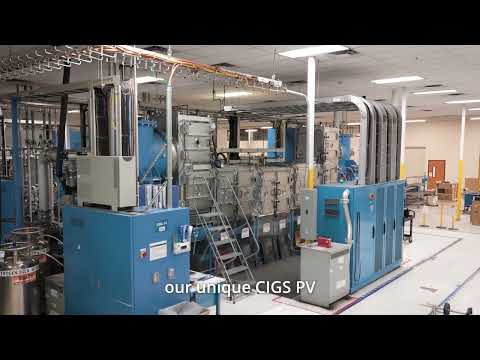
The energy sector is witnessing significant momentum, particularly in photovoltaics and battery technology. First Solar, Inc. is actively scaling its thin-film cadmium telluride (CdTe) solar module production, underscoring the role of quasivacuum sputtering and vapor transport deposition in achieving cost-effective, high-efficiency solar panels. Similarly, Panasonic Corporation has integrated quasivacuum thin film deposition in the fabrication of next-generation lithium-ion batteries, focusing on solid-state electrolyte layers that enhance safety and energy density.
Beyond traditional sectors, quasivacuum thin films are being explored for advanced packaging, biomedical devices, and quantum technology. Research initiatives at organizations like Fraunhofer Society are targeting bioactive coatings for implants and hermetic barriers for quantum chips, areas where film uniformity and interface engineering are critical.
Looking ahead, the outlook for quasivacuum thin film manufacturing remains robust. The convergence of automation, real-time process monitoring, and novel material precursors is set to further expand the range of applications and improve manufacturability. As companies and research institutes continue to push the boundaries of thin film performance, the impact on electronics, optics, energy, and beyond will likely deepen in the next several years.
Investment Trends and Funding Hotspots
Quasivacuum thin film manufacturing, which leverages low-pressure environments for more efficient and scalable deposition processes, is emerging as a focal point for strategic investments and funding allocations in 2025. As demand intensifies for advanced thin films in sectors such as semiconductors, energy storage, and flexible electronics, capital flows are increasingly channeled toward companies and research institutes pioneering next-generation quasivacuum deposition technologies.
In 2025, significant investment activity is centered in East Asia, particularly South Korea and Japan, where leading manufacturers are expanding capacity for new thin film materials and equipment. Samsung SDI and LG Chem continue to allocate substantial R&D budgets toward the development of advanced thin film batteries and display technologies, with quasivacuum systems cited as a cornerstone of their process innovation strategies. In Japan, ULVAC, Inc. is investing in the commercialization of new quasivacuum sputtering equipment, targeting both domestic and export markets.
Europe remains a hub for collaborative projects and public–private partnerships. The European Union’s Horizon Europe program has earmarked funds for thin film innovation projects, and manufacturers such as Oxford Instruments and EV Group are recipients of these grants, channeling the capital into scaling up quasivacuum platforms for applications in photovoltaics and photonics. These investments are frequently accompanied by strategic alliances with universities and national research organizations.
In the United States, venture capital and government incentives are catalyzing the growth of startups focused on scalable, energy-efficient thin film production. Applied Materials has announced increased investment in its thin film deposition portfolio, with a particular emphasis on quasivacuum solutions for next-generation semiconductor nodes. Similarly, First Solar is channeling new funding into advancing its cadmium telluride (CdTe) thin film processes, citing quasivacuum deposition as a key enabler.
Looking ahead, funding hotspots are projected to align with the rollout of advanced electronics, solid-state batteries, and green energy initiatives. As supply chain resilience and sustainability remain top priorities, investment in quasivacuum thin film manufacturing is expected to accelerate, with both established players and emerging enterprises securing new rounds of funding through 2026 and beyond.
Supply Chain Challenges and Solutions
The manufacturing of quasivacuum thin films—crucial for advanced electronics, photovoltaics, and optical coatings—faces persistent supply chain challenges as the sector moves through 2025. These challenges stem from global material shortages, logistical disruptions, and technological dependencies, but innovative responses are emerging across the industry.
A primary concern is the procurement of high-purity source materials such as sputtering targets (e.g., indium, gallium, rare earths) and specialty substrates. Prolonged disruptions from geopolitical tensions and supply bottlenecks, particularly in Asia, have led manufacturers like Tosoh Corporation and Hanwha Group to diversify sourcing and invest in direct supply agreements with upstream mines and refiners. These strategies have mitigated some volatility in raw material pricing, but intermittent shortages remain a risk.
Specialized equipment, such as advanced deposition systems (magnetron sputtering, atomic layer deposition, and e-beam evaporation), represents another vulnerability. Lead times for critical components—vacuum pumps, precision gauges, and process control modules—have lengthened since the COVID-19 pandemic, with suppliers like Pfeiffer Vacuum Technology AG and Edwards Vacuum reporting continued high demand and expanded order backlogs through early 2025. In response, manufacturers are increasingly engaging in collaborative development agreements to secure priority access, co-developing next-generation tools with OEMs to accelerate innovation and ensure supply.
Additionally, the logistics of thin film manufacturing—sensitive both to contamination and environmental controls—require specialized packaging and rapid shipment. Companies such as Umicore have expanded regional distribution hubs in North America and Europe to reduce transit times and environmental risks, while also piloting digital tracking for critical shipments to enhance transparency and reliability.
On the solutions front, digitalization and predictive analytics are being rapidly adopted to optimize inventory management and forecast disruptions. Covestro AG and others have invested in AI-driven supply chain platforms that integrate supplier data and machine learning to flag potential shortages before they impact production. Furthermore, sustainability pressures and regulatory requirements are driving the adoption of recycling and closed-loop sourcing, with firms like DuPont increasing the use of recovered materials in their thin film product lines.
Looking ahead, as demand for quasivacuum thin films grows across sectors—from OLED displays to next-generation batteries—the industry’s resilience will depend on continued innovation in materials sourcing, equipment partnerships, logistics, and digital supply chain management. While significant risks persist, the accelerated pace of collaborative solutions suggests a more robust and responsive ecosystem is emerging for 2025 and beyond.
Regulatory & Environmental Considerations
As quasivacuum thin film manufacturing accelerates across electronics, optics, and energy sectors, regulatory and environmental considerations are increasingly integral to technology deployment and supply chain strategy. In 2025, compliance with global standards for emissions control, chemical use, and waste management is shaping manufacturing practices and investments.
Many processes in quasivacuum thin film manufacturing—such as sputtering, evaporation, and atomic layer deposition—require the use of hazardous chemicals, high energy consumption, and specialized vacuum systems. Regulatory agencies, including the United States Environmental Protection Agency and the European Chemicals Agency, have established stringent guidelines for permissible exposure limits, emissions of volatile organic compounds (VOCs), and end-of-life treatment of thin film devices, especially those containing rare earth elements or heavy metals.
Manufacturers are responding with a dual approach: process innovation for greener operations and investment in environmental monitoring. For example, ULVAC, Inc. and Oxford Instruments are developing deposition systems that minimize byproducts and energy usage, while integrating abatement technologies for exhaust gases. In 2024, VON ARDENNE GmbH introduced new vacuum coating platforms featuring improved solvent recovery and resource efficiency, targeting compliance with both European REACH directives and the Restriction of Hazardous Substances (RoHS) rules.
Recycling and circularity are emerging as focal points. Thin film photovoltaic producers such as First Solar, Inc. have established closed-loop recycling programs for end-of-life modules, directly addressing regulatory demands for responsible waste handling and material recovery. In Asia, manufacturers like Applied Materials, Inc. are collaborating with local regulators to pilot water recycling and zero-liquid-discharge systems, reflecting the growing importance of water stewardship in semiconductor thin film fabrication.
Looking ahead, regulatory frameworks are expected to intensify. The European Union is considering extending Ecodesign and digital product passport requirements to electronics containing thin films, which would impact traceability and reporting obligations through the supply chain. The semiconductor sector anticipates further rules on perfluorinated compound (PFC) emissions and stricter lifecycle carbon accounting, likely influencing capital investments in new equipment and retrofit projects.
In sum, as the industry moves through 2025 and beyond, proactive alignment with evolving regulations—particularly around emissions, hazardous materials, and resource efficiency—will be central to global competitiveness and environmental stewardship in quasivacuum thin film manufacturing.
Future Outlook: Game-Changers and Strategic Roadmaps
Quasivacuum thin film manufacturing—leveraging controlled, low-pressure environments distinct from ultra-high-vacuum systems—has emerged as a transformative approach for fabricating advanced electronics, optoelectronics, and energy devices. As of 2025, the sector is witnessing accelerated investment and technological pivots, with stakeholders targeting greater scalability, cost-effectiveness, and sustainability.
Key players such as Oxford Instruments and Plassys Bestek are expanding their portfolios to include modular deposition systems that enable precise control of film thickness and uniformity while reducing energy requirements versus traditional high-vacuum solutions. These advances address the growing demand for thin films in flexible displays, high-efficiency photovoltaics, and next-generation semiconductors.
In 2025, the drive toward gigafactory-scale production is prompting both equipment makers and materials suppliers to collaborate on integrated process lines. For instance, ULVAC, Inc. is focusing on hybrid systems that combine quasivacuum and atmospheric techniques to cut manufacturing time and costs for large-area organic electronics. Such developments are strategically aligned with the global push for electrification and digitalization, where thin film innovation underpins performance and miniaturization.
Sustainability is also at the forefront. Manufacturers like EV Group are emphasizing low-carbon footprint materials and recycling of process gases in their latest equipment offerings. These efforts are in response to increasing regulatory and customer demands for greener supply chains, particularly in sectors such as solar energy and advanced packaging.
Looking ahead to the next few years, the outlook is shaped by several game-changers:
- Ongoing miniaturization in microelectronics, demanding ever-thinner, defect-free films with atomic-level precision, is catalyzing R&D into in-situ diagnostics and AI-driven process optimization.
- Emergence of novel materials, such as 2D semiconductors and perovskites, is expanding the scope of quasivacuum deposition beyond conventional silicon-based devices.
- Strategic partnerships—such as those between Oxford Instruments and leading semiconductor foundries—are accelerating technology transfer from pilot lines to mass production.
As 2025 progresses, the convergence of automation, materials innovation, and sustainable engineering is set to define the competitive landscape. Companies able to deliver robust, adaptive quasivacuum thin film platforms will be well-positioned to shape the next wave of electronics and energy markets.
Sources & References
- Oxford Instruments
- ULVAC
- SINGULUS TECHNOLOGIES
- EV Group
- Bühler Group
- Pfeiffer Vacuum
- Leybold
- Air Liquide
- Advanced Micro-Fabrication Equipment Inc. (AMEC)
- Tokyo Ohka Kogyo Co., Ltd.
- Oxford Instruments plc
- Carl Zeiss AG
- First Solar, Inc.
- Fraunhofer Society
- ULVAC, Inc.
- Edwards Vacuum
- Umicore
- Covestro AG
- DuPont
- European Chemicals Agency
- VON ARDENNE GmbH
- Plassys Bestek